

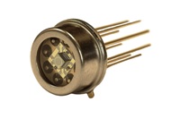
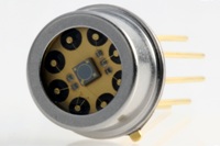
TO Style Package
Centeral PD + surrounding LEDs
1.7 µm-class: one monolithic InGaAs die divided into four quadrants
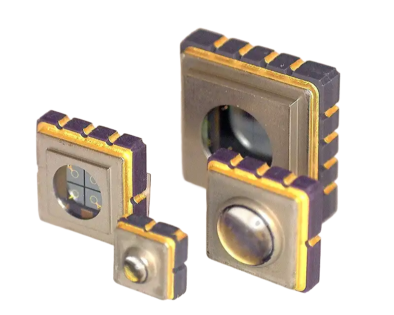
2.6 µm-class: four discrete extended-InGaAs detector elements in a 2 x 2 arrangement
LED wavelength options
Detector options up to ~2.6 µm
Custom multi-chip packaging
LATHAM, NEW YORK – September, 2026 – Optrans America Corporation today announced an expanded family of custom multi-wavelength LED and photodiode packages that combine multiple optical emitters and a photodetector within a single compact device.
The platform can place a Si, SiC or InGaAs photodiode at the center of the package with multiple LED chips arranged around it. LED wavelengths can be selected from approximately 235nm to 2300 nm, covering ultraviolet, visible, near-infrared and short-wave infrared regions. Multiple photodiode chip sizes are available, including Si, SiC, standard InGaAs and extended-InGaAs detector options with cutoff wavelengths up to approximately 2.6 µm.
Representative TO-style and surface-mount package configurations
Multi-wavelength optical instruments often require several emitters together with a photodetector to measure reflected, transmitted, scattered or absorbed light. Using individually packaged LEDs and a separate detector can increase board space, optical alignment requirements and the number of components in the optical head. Optrans‘ multi-chip packaging approach integrates these functions into a single configurable package, simplifying optical geometry and enabling compact application-specific sensor designs.
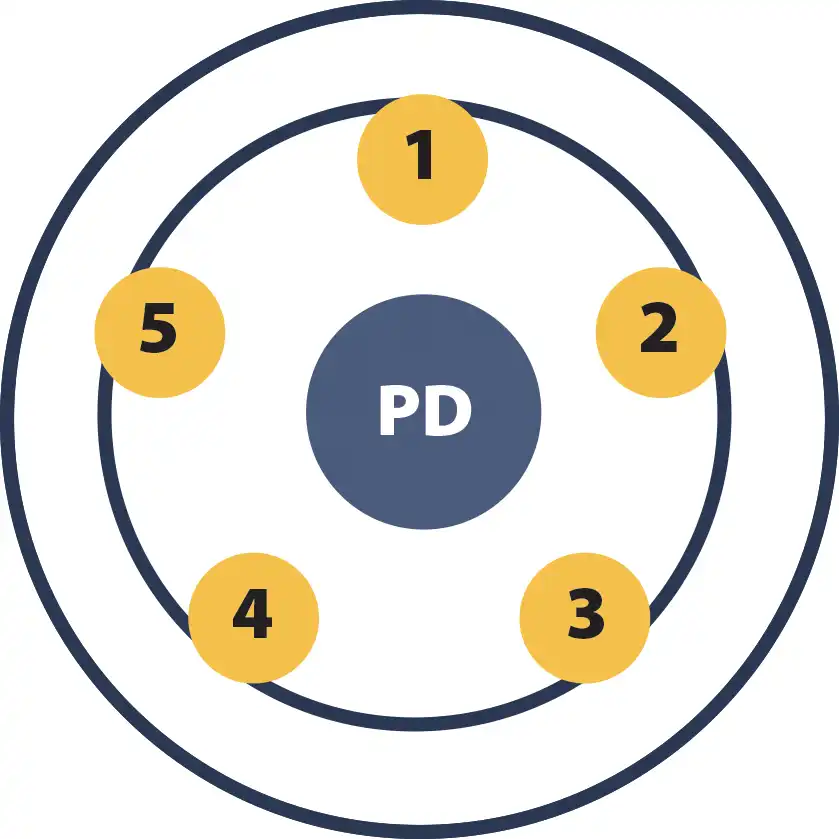
1 photodiode + up to 5 LEDs

1 photodiode + up to 4 LEDs
For TO-style metal-can packages, Optrans can integrate one centrally positioned photodiode with up to five LED chips. When a photodiode is not required, up to seven LED chips can be installed in the package. Each emitter wavelength can be selected according to the optical requirements of the application.
For compact PCB assemblies, Optrans offers a 7.24 mm square seam-welded surface-mount platform. The SMD configuration can integrate one photodiode plus up to four LED chips, providing a compact source-and-detector solution suitable for high-density designs and automated assembly.
Representative configurations are shown to illustrate packaging flexibility; final wavelength combinations and detector selections are application-specific.
| Example | Package | Photodiode | LED configuration |
|---|---|---|---|
| ILAM1319L38-SU | TO style | PD2601 | 1300 / 1460 / 1650 / 1720 / 1900 nm |
| ILAM141719L38-SU | TO style | PD2601 | 1460 / 1720 / 1900 nm |
| ILA8123L38-SU | TO style | None | 7 LEDs: 810 / 1040 / 1200 / 1460 / 1550 / 1720 / 2300 nm |
| ILAM1319SMSFY3 | 7.24 mm SMD | PD2601 | 1300 / 1460 / 1720 / 1900 nm |
| ILAM10415SMSFY3 | 7.24 mm SMD | PD1300 | 1040 / 1300 / 1460 / 1550 nm |
Representative configurations are shown to illustrate packaging flexibility; final wavelength combinations and detector selections are application-specific.
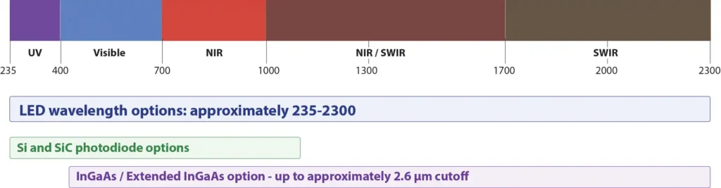
The detector element can be selected according to the required spectral range, sensitivity, response speed and optical geometry. Optrans can provide Si or SiC photodiodes for ultraviolet, visible and near-infrared applications, as well as standard and extended InGaAs photodiodes for near-infrared and SWIR applications. Extended-InGaAs detector options are available with cutoff wavelengths up to approximately 2.6 µm. Multiple chip sizes and active-area options are available to balance sensitivity, alignment tolerance and package constraints.
The integrated Multi-LED + Photodiode platform is intended for optical systems that benefit from discrete multi-wavelength illumination and a closely located detector. Potential applications include: Extended-InGaAs detector options are available with cutoff wavelengths up to approximately 2.6 µm. Multiple chip sizes and active-area options are available to balance sensitivity, alignment tolerance and package constraints.
Rather than limiting customers to a fixed emitter-and-detector combination, Optrans can configure the optical package according to the requirements of each application. Customers can specify LED wavelengths, the number of emitters, photodiode technology, detector chip size, active area, package type, optical window or lens, electrical pin configuration and chip placement.
Optrans America Corporation will continue to expand its multi-chip optoelectronic packaging capabilities by combining LEDs, photodiodes and other optical semiconductor devices within increasingly compact package formats. By integrating light sources and detectors into a single customizable package, Optrans aims to help customers reduce component count, simplify optical design and accelerate development of next-generation analytical, medical, industrial and sensing equipment.
Optrans America Corporation
Latham, New York, USA
Email: in**@************ca.com
Product configurations and specifications may vary according to wavelength, detector type, chip size and package configuration. Final specifications should be confirmed for each customer application.